Main Menu
- Home
- Product Finder
- Calibration Systems
- Calibration Services
- Digital Sensing
- Industrial Vibration Calibration
- Modal and Vibration Testing
- Non-Destructive Testing
- Sound & Vibration Rental Program
- Learn
- About Us
- Contact Us
1. Impedance conversion
2. Signal normalization
3. Gain adjust
All three are common to both charge and voltage output systems.
The method of accomplishing and location of each function in the voltage output system often results in improved performance and significantly lower cost per channel.
The basic function of any piezoelectric sensor signal conditioner is to convert the high impedance charge output from a crystal to a usable low impedance voltage signal for digitization storage and/or analysis purposes.
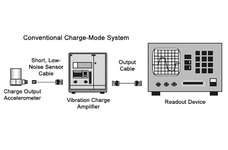
In a charge output sensor, impedance conversion is accomplished remotely from the sensor by a high gain capacitive feedback amplifier which effectively short circuits the high impedance piezoelectric crystal, thereby dumping the charge signal into a feedback capacitor and providing a low impedance output voltage signal.
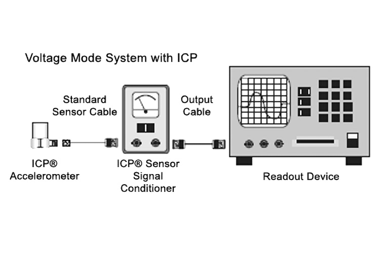
In a voltage output sensor, impedance conversion is accomplished internal to the sensor by a micro-electronic amplifier which converts the high impedance charge signal directly into a useful low impedance voltage signal.
The resolution (noise floor) of the charge mode system is a variable. It is dependent on the capacitive loading of the accelerometer and input cable connecting the signal to the input of the charge amplifier. Because of this effect, low-level measurements are difficult to make using long input cables. Technicians counter this problem by locating the charge amplifier closer to the accelerometer to improve the signal/noise ratio. In effect, this simply accomplishes the charge to voltage conversion closer to the sensor and lowers noise by reducing capacitive loading on the charge amplifier input. There are also other environmental considerations that affect the noise on the measurement signal including: triboelectric noise from cable whip, and loss of insulation resistance by contamination of connectors (in the high impedance chain) by grease, dirt or oil.
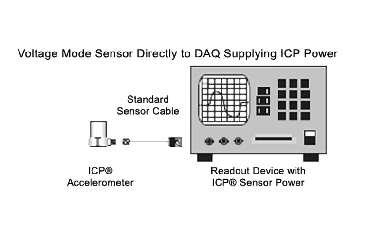
The voltage output sensor alleviates these issues by simply placing the impedance conversion electronics inside the accelerometer. This minimizes noise, seals all high impedance circuitry inside the accelerometer, and allows the use of long, low cost, ordinary coaxial cable without increase in noise or loss of excellent inherent resolution characteristics of a piezoelectric sensor.
A) Laboratory charge amplifiers usually have a ten-turn pot to enter charge sensitivity of the sensor.
B) In some voltage mode accelerometers, normalization is accomplished inside the accelerometer by manufacturing process and precision (either mechanically, electrically, or both). Variable gain adjust is also available in most ICP® power units to normalize output for non standard accelerometers.
Normalization is accomplished by controlling the tolerances on the mass inside the accelerometer. This simplifies operation, minimizes record keeping, and facilitates interchangeability of accelerometers in the measurement system without making circuit adjustments.
Gain Adjustment
A) Laboratory type charge amplifiers have a very specialized high impedance gain adjust circuitry.
B) Voltage mode accelerometers use the gain already available in many readout instruments. (If gain is required, as may be required for tape recording, any standard voltage amplifier may be used or low cost power unit with gain. In most modern 24-bit dynamic signal analyzers no gain is needed at all.)
In many charge mode systems gain adjust in both the charge amplifier and readout instrument is redundant.
In the modern voltage mode system illustrated, gain adjust is provided in the readout instrument. If gain is needed, low cost gain can be obtained from standard instrumentation amplifiers or power units with built-in gain.


